Automated Optical Inspection/wafer surface inspection system/YGK Corporation
TEL. +81-55-284-6866
595-2,Kuruwada Minami-Alps,Yamanashi 400-0311,Japan
PRODUCTS
YPI−MX−Θ DC
- 【New development】
Wafer surface inspection system for SiC/GaN.
Driving dual laser head for SiC surface particle scanner【YPI-MX-θ DC】
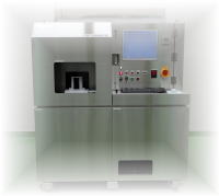 YPI-MX-θ DC can measure not just SiC wafer but also a transparent wafer,Si
wafer and LT wafer. Maximum sensitivity is 0.1μm PSL.
YPI-MX-θ DC can measure not just SiC wafer but also a transparent wafer,Si
wafer and LT wafer. Maximum sensitivity is 0.1μm PSL.
4inch SiC wafer is measured within 5min. The result measurement includes a latent scratch information.
Click ⇒
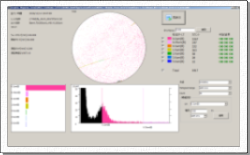
LT wafer measurement result example
YPI−MN
- Compact・high performance wafer surface inspection system.
The wafer surface particle scanner【YPI-MN】
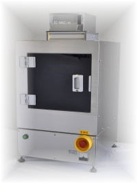
Transparent substrate is capable measurement 0.3um.
The measurement size is capable until 200mm. (Conditional)
Click ⇒
このページの先頭へ/ b 2
バナースペース
YGK Corporation
595-2,Kuruwada Minami-Alps,
Yamanashi 400-0311,japan
TEL +81-55-284-6866
FAX +81-55-284-6867