Automated Optical Inspection/wafer surface inspection system/YGK Corporation
TEL. +81-55-284-6866
595-2,Kuruwada Minami-Alps,Yamanashi 400-0311,Japan
YPI−MX−Θ DCFor SiN wafer, GaN wafer, or transparent wafer.

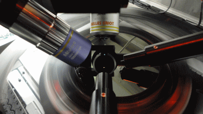
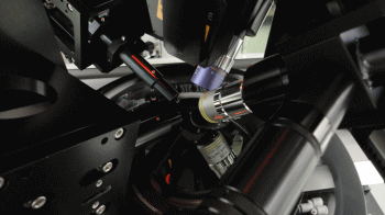
- New designed detection units which are cross
setting with dual 355nm (UV) laser.
The dual detector contributes enhanced detection for a slight scratch generated directional light scattered compared with conventional particle inspection system.
And also, 355nm laser is effective for isolated detection of SiC surface only.
Inspection time is within 5min for 4inch SiC wafer.


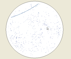
dual laser units Inspection result image
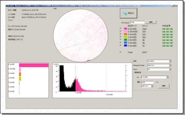
- Transparent wafer, silicon wafer or LT wafer can be measured by YPI-MX-θDC. Maximum sensitivity is 0.1μm.

MAP result for LT wafer
Approx 2minutes inspection time for 4inch LT wafer.
Specifications
- Scanning method
- Rotation or XY scanning with dual laser units
- Work piece setting
- Manual or Auto loading (Cassette to Cassette)
- Electric consumption
- AC100V/200V 30A
- Maximum sensitivity
- 0.1μm
- Reproducibility
- σ/X≦10%
- Inspection time
- Within 2 minutes for 4inch wafer
- Target substrate and wafer
- SiC wafer、GaN wafer、LT wafer、film deposited wafer、
Transparent substrate and wafer - Appearance Dimension
- W900mm×D1,000mm×H1,757mm(Manual)
W1,530mm×D1,200mm×H1,715mm(Auto loading) - Weight
- Approx.500kg(Manual)
Approx.1000kg(Auto loading)
バナースペース
YGK Corporation
595-2,Kuruwada Minami-Alps,
Yamanashi 400-0311,japan
TEL +81-55-284-6866
FAX +81-55-284-6867