Automated Optical Inspection/wafer surface inspection system/YGK Corporation
TEL. +81-55-284-6866
595-2,Kuruwada Minami-Alps,Yamanashi 400-0311,Japan
Develop Full Surface Defect Inspection Technology for Sic Wafers
Used to Make Power Semiconductors
- High-speed imaging technology contributes to higher quality SiC wafers -
September 9, 2022
Kwansei Gakuin University
Toyota Tsusho Corporation
YGK Corporation
Kwansei Gakuin Educational Foundation (“Kwansei Gakuin University”), Toyota Tsusho Corporation (“Toyota Tsusho”), and YGK Corporation (“YGK”) announced today that they have jointly developed an inspection technology for sub-surface damage (SSD*) that occurs in the manufacturing process of silicon carbide (SiC) wafers for power semiconductors. This innovative inspection technology is one of the outcomes of a collaboration between Kwansei Gakuin University and Toyota Tsusho, initially launched in 2017, to jointly develop mass production processing technologies for high-quality SiC wafers. It is expected to improve production efficiency and to address problems faced on the frontline of semiconductor production and research.
1. Background
SiC is a next-generation power semiconductor material to dramatically reduce
power loss, compared to
silicon (Si), as a popular power semiconductor material. For this reason,
it is expected to be adopted
much more in the future to achieve carbon neutrality in automotive, railway,
industrial machinery,
power and other industries. Expectations are particularly high for electric
vehicles (EVs, HEVs, FCEVs).
One issue with SiC wafer production is that, due the hard and brittle nature
of the material, the crystal
layer near the surface can be fractured and SSD is formed when slicing
and grinding/polishing the
wafers (see figure 1). While the SSD reduces the yield rate of wafer production and causes defects of
power semiconductor, there was a lack of technologies available for imaging
the full wafer surface.
Therefore, there was a strong desire for high-speed, high-precision SSD
inspection technologies that
could be used for quality management during the wafer mass production process, and that could also be
applied to acceptance inspections.
2. Joint Development
Kwansei Gakuin University (Professor Tadaaki Kaneko, School of Engineering)
and Toyota Tsusho
turned their attention to the applied laser light scattering technology of YGK. Together, the three
organizations developed a technology for the full surface imaging of the
SSD created in the
machining process of SiC wafers, and enabling relative comparisons of the
wafer quality.
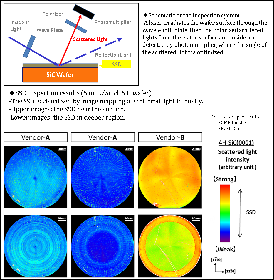
This technology enables imaging of the SSD by irradiating wafer surface
with laser light and then
detecting, at the optimal angle, light scattered from the surface and internally (see figure 2). It also
enables high-speed inspection of the full wafer surface, which means it
can be applied to operations
like quality management in the mass production process. The aim now is
to move quickly to
commercialization of wafer inspection devices equipped with this technology.
Incidentally, the SSD confirmed through this inspection technology can
be completely eliminated by
using “Dynamic AGE-ing®,” which is a contactless nano process technology
integrating thermal
etching and crystal growth, allowing control at the nanometer level. (Dynamic AGE-ing was
announced by Kwansei Gakuin University and Toyota Tsusho in March 2021.)
This new technology will also be officially announced and exhibited at
the International Conference
on Silicon Carbide and Related Materials 2022 (ICSCRM 2022) to be held
September 11–16, 2022,
in Switzerland.
* SSD is created by contact with abrasives and stress, etc., during mechanical
processing of wafers
(slicing, grinding, and polishing).
Figure 1. Overview of SiC wafer manufacturing
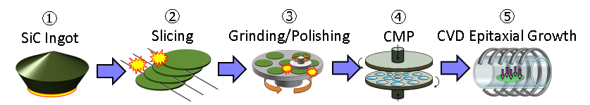
*CMP=Chemical Mechanical Polish
<Issues>
・Machining processes (②,③) introduce the sub-surface damage (SSD) at the SiC substrate surface.
・The SSD may remain after CMP (④).
・The pretreatment of CVD epitaxial growth (⑤) may not remove the SSD completely,
which may
cause product defects.
・Conventional inspection methods have difficulties to detect the actual state of the SSD.
Figure 2. Overview of SSD inspection method
バナースペース
YGK Corporation
595-2,Kuruwada Minami-Alps,
Yamanashi 400-0311,japan
TEL +81-55-284-6866
FAX +81-55-284-6867